Keon+Jae+Lee
-
 A KAIST Team Develops Selective Transfer Printing Technology for MicroLEDs
- A KAIST research team led by Professor Keon Jae Lee demonstrates the transfer printing of a large number of micro-sized inorganic semiconductor chips via the selective modulation of micro-vacuum force.
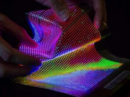
MicroLEDs are a light source for next-generation displays that utilize inorganic LED chips with a size of less than 100 μm. MicroLEDs have attracted a great deal of attention due to their superior electrical/optical properties, reliability, and stability compared to conventional displays such as LCD, OLED, and QD. To commercialize microLEDs, transfer printing technology is essential for rearranging microLED dies from a growth substrate onto the final substrate with a desired layout and precise alignment. However, previous transfer methods still have many challenges such as the need for additional adhesives, misalignment, low transfer yield, and chip damage.
Professor Lee’s research team has developed a micro-vacuum assisted selective transfer printing (µVAST) technology to transfer a large number of microLED chips by adjusting the micro-vacuum suction force.
The key technology relies on a laser-induced etching (LIE) method for forming 20 μm-sized micro-hole arrays with a high aspect ratio on glass substrates at fabrication speed of up to 7,000 holes per second. The LIE-drilled glass is connected to the vacuum channels, controlling the micro-vacuum force at desired hole arrays to selectively pick up and release the microLEDs. The micro-vacuum assisted transfer printing accomplishes a higher adhesion switchability compared to previous transfer methods, enabling the assembly of micro-sized semiconductors with various heterogeneous materials, sizes, shapes, and thicknesses onto arbitrary substrates with high transfer yields.
< Figure 01. Concept of micro-vacuum assisted selective transfer printing (μVAST). >
Professor Keon Jae Lee said, “The micro-vacuum assisted transfer provides an interesting tool for large-scale, selective integration of microscale high-performance inorganic semiconductors. Currently, we are investigating the transfer printing of commercial microLED chips with an ejector system for commercializing next-generation displays (Large screen TVs, flexible/stretchable devices) and wearable phototherapy patches.”
This result titled “Universal selective transfer printing via micro-vacuum force” was published in Nature Communications on November 26th, 2023. (DOI: 10.1038/S41467-023-43342-8)
< Figure 02. Universal transfer printing of thin-film semiconductors via μVAST. >
< Figure 03. Flexible devices fabricated by μVAST. >
Title: Entire process including LIE and µVAST
Vimeo link: https://vimeo.com/894430416?share=copy
2023.12.19 View 1141
A KAIST Team Develops Selective Transfer Printing Technology for MicroLEDs
- A KAIST research team led by Professor Keon Jae Lee demonstrates the transfer printing of a large number of micro-sized inorganic semiconductor chips via the selective modulation of micro-vacuum force.
MicroLEDs are a light source for next-generation displays that utilize inorganic LED chips with a size of less than 100 μm. MicroLEDs have attracted a great deal of attention due to their superior electrical/optical properties, reliability, and stability compared to conventional displays such as LCD, OLED, and QD. To commercialize microLEDs, transfer printing technology is essential for rearranging microLED dies from a growth substrate onto the final substrate with a desired layout and precise alignment. However, previous transfer methods still have many challenges such as the need for additional adhesives, misalignment, low transfer yield, and chip damage.
Professor Lee’s research team has developed a micro-vacuum assisted selective transfer printing (µVAST) technology to transfer a large number of microLED chips by adjusting the micro-vacuum suction force.
The key technology relies on a laser-induced etching (LIE) method for forming 20 μm-sized micro-hole arrays with a high aspect ratio on glass substrates at fabrication speed of up to 7,000 holes per second. The LIE-drilled glass is connected to the vacuum channels, controlling the micro-vacuum force at desired hole arrays to selectively pick up and release the microLEDs. The micro-vacuum assisted transfer printing accomplishes a higher adhesion switchability compared to previous transfer methods, enabling the assembly of micro-sized semiconductors with various heterogeneous materials, sizes, shapes, and thicknesses onto arbitrary substrates with high transfer yields.
< Figure 01. Concept of micro-vacuum assisted selective transfer printing (μVAST). >
Professor Keon Jae Lee said, “The micro-vacuum assisted transfer provides an interesting tool for large-scale, selective integration of microscale high-performance inorganic semiconductors. Currently, we are investigating the transfer printing of commercial microLED chips with an ejector system for commercializing next-generation displays (Large screen TVs, flexible/stretchable devices) and wearable phototherapy patches.”
This result titled “Universal selective transfer printing via micro-vacuum force” was published in Nature Communications on November 26th, 2023. (DOI: 10.1038/S41467-023-43342-8)
< Figure 02. Universal transfer printing of thin-film semiconductors via μVAST. >
< Figure 03. Flexible devices fabricated by μVAST. >
Title: Entire process including LIE and µVAST
Vimeo link: https://vimeo.com/894430416?share=copy
2023.12.19 View 1141 -
 KAIST Team Develops Highly-Sensitive Wearable Piezoelectric Blood Pressure Sensor for Continuous Health Monitoring
- A collaborative research team led by KAIST Professor Keon Jae Lee verifies the accuracy of the highly-sensitive sensor through clinical trials
- Commercialization of the watch and patch-type sensor is in progress
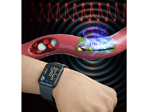
A KAIST research team led by Professor Keon Jae Lee from the Department of Materials Science and Engineering and the College of Medicine of the Catholic University of Korea has developed a highly sensitive, wearable piezoelectric blood pressure sensor.
Blood pressure is a critical indicator for assessing general health and predicting stroke or heart failure. In particular, cardiovascular disease is the leading cause of global death, therefore, periodic measurement of blood pressure is crucial for personal healthcare.
Recently, there has been a growing interest in healthcare devices for continuous blood pressure monitoring. Although smart watches using LED-based photoplethysmography (PPG) technology have been on market, these devices have been limited by the accuracy constraints of optical sensors, making it hard to meet the international standards of automatic sphygmomanometers.
Professor Lee’s team has developed the wearable piezoelectric blood pressure sensor by transferring a highly sensitive, inorganic piezoelectric membrane from bulk sapphire substrates to flexible substrates. Ultrathin piezoelectric sensors with a thickness of several micrometers (one hundredth of the human hair) exhibit conformal contact with the skin to successfully collect accurate blood pressure from the subtle pulsation of the blood vessels.
Clinical trial at the St. Mary’s Hospital of the Catholic University validated the accuracy of blood pressure sensor at par with international standard with errors within ±5 mmHg and a standard deviation under 8 mmHg for both systolic and diastolic blood pressure. In addition, the research team successfully embedded the sensor on a watch-type product to enable continuous monitoring of blood pressure.
Prof. Keon Jae Lee said, “Major target of our healthcare devices is hypertensive patients for their daily medical check-up. We plan to develop a comfortable patch-type sensor to monitor blood pressure during sleep and have a start-up company commercialize these watch and patch-type products soon.”
This result titled “Clinical validation of wearable piezoelectric blood pressure sensor for health monitoring” was published in the online issue of Advanced Materials on March 24th, 2023. (DOI: 10.1002/adma.202301627)
Figure 1. Schematic illustration of the overall concept for a wearable piezoelectric blood pressure sensor (WPBPS).
Figure 2. Wearable piezoelectric blood pressure sensor (WPBPS) mounted on a watch (a) Schematic design of the WPBPS-embedded wristwatch. (b) Block diagram of the wireless communication circuit, which filters, amplifies, and transmits wireless data to portable devices. (c) Pulse waveforms transmitted from the wristwatch to the portable device by the wireless communication circuit. The inset shows a photograph of monitoring a user’s beat-to-beat pulses and their corresponding BP values in real time using the developed WPBPS-mounted wristwatch.
2023.04.17 View 2835
KAIST Team Develops Highly-Sensitive Wearable Piezoelectric Blood Pressure Sensor for Continuous Health Monitoring
- A collaborative research team led by KAIST Professor Keon Jae Lee verifies the accuracy of the highly-sensitive sensor through clinical trials
- Commercialization of the watch and patch-type sensor is in progress
A KAIST research team led by Professor Keon Jae Lee from the Department of Materials Science and Engineering and the College of Medicine of the Catholic University of Korea has developed a highly sensitive, wearable piezoelectric blood pressure sensor.
Blood pressure is a critical indicator for assessing general health and predicting stroke or heart failure. In particular, cardiovascular disease is the leading cause of global death, therefore, periodic measurement of blood pressure is crucial for personal healthcare.
Recently, there has been a growing interest in healthcare devices for continuous blood pressure monitoring. Although smart watches using LED-based photoplethysmography (PPG) technology have been on market, these devices have been limited by the accuracy constraints of optical sensors, making it hard to meet the international standards of automatic sphygmomanometers.
Professor Lee’s team has developed the wearable piezoelectric blood pressure sensor by transferring a highly sensitive, inorganic piezoelectric membrane from bulk sapphire substrates to flexible substrates. Ultrathin piezoelectric sensors with a thickness of several micrometers (one hundredth of the human hair) exhibit conformal contact with the skin to successfully collect accurate blood pressure from the subtle pulsation of the blood vessels.
Clinical trial at the St. Mary’s Hospital of the Catholic University validated the accuracy of blood pressure sensor at par with international standard with errors within ±5 mmHg and a standard deviation under 8 mmHg for both systolic and diastolic blood pressure. In addition, the research team successfully embedded the sensor on a watch-type product to enable continuous monitoring of blood pressure.
Prof. Keon Jae Lee said, “Major target of our healthcare devices is hypertensive patients for their daily medical check-up. We plan to develop a comfortable patch-type sensor to monitor blood pressure during sleep and have a start-up company commercialize these watch and patch-type products soon.”
This result titled “Clinical validation of wearable piezoelectric blood pressure sensor for health monitoring” was published in the online issue of Advanced Materials on March 24th, 2023. (DOI: 10.1002/adma.202301627)
Figure 1. Schematic illustration of the overall concept for a wearable piezoelectric blood pressure sensor (WPBPS).
Figure 2. Wearable piezoelectric blood pressure sensor (WPBPS) mounted on a watch (a) Schematic design of the WPBPS-embedded wristwatch. (b) Block diagram of the wireless communication circuit, which filters, amplifies, and transmits wireless data to portable devices. (c) Pulse waveforms transmitted from the wristwatch to the portable device by the wireless communication circuit. The inset shows a photograph of monitoring a user’s beat-to-beat pulses and their corresponding BP values in real time using the developed WPBPS-mounted wristwatch.
2023.04.17 View 2835 -
 KAIST Team Develops Surface-Lighting MicroLED Patch with Significant Melanogenesis Inhibition Effect
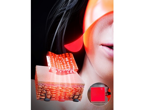
A KAIST research team led by Ph.d candidate Jae Hee Lee and Professor Keon Jae Lee from the Department of Materials Science and Engineering has developed a surface-lighting microLED patch for UV-induced melanogenesis inhibition.
Melanin is brown or dark pigments existing in the skin, which can be abnormally synthesized by external UV or stress. Since the excessive melanin leads to skin diseases such as spots and freckles, proper treatment is required to return normal skin condition.
Recently, LED-based photo-stimulators have been released for skin care, however, their therapeutic effect is still controversial. Since conventional LED stimulators cannot conformally attach to the human skin, distance-induced side effects are caused by light loss and high heat transfer. To achieve effective phototreatment, the LED stimulator needs to be irradiated in contact with the human skin surface, enabling proper and uniform light deliver to the dermis with minimal optical loss.
In this work, the research team fabricated skin-attachable surface-lighting microLED (SµLED, 4 × 4 cm2) patch by utilizing a thousand of microLED chips and silica-embedded light diffusion layer. 100 µm-sized LED chips are vertically-interconnected for high flexibility and low heat generation, allowing its long-term operation on the human skin.
< Image 1. The overall concept of SµLED patch. a) SµLED patch operated on the human skin. b) Schematic illustration of SµLED patch structure. c) 4 × 4 cm2-sized SµLED patch. d) Schematic illustration of the advantages of SµLED patch such as efficient light delivery, low heat generation, and surface-lighting irradiation. >
The research team confirmed melanogenesis inhibition by irradiating the SµLED patch and the conventional LED (CLED) on the artificial human skin and mice dorsal skin. The SµLED-treated groups of human cells and mouse tissues showed minimal epidermal photo-toxicity and consistently effective reduction in synthesized melanin, compared to CLED-treated groups. In addition, significant suppression of proteins/catalysts expression involved in melanin synthesis such as MITF (microphthalmia-associated transcription factor), Melan-A and tyrosinase was verified.
< Image 2. The efficacy of melanogenesis inhibition on 3D human skin cells. a). Different irradiation conditions for a-MSH (major factor to stimulate melanin synthesis) treated cells. b) The ratio of pigmented area to total epidermis area. c) Relative variance of melanin level in 1 cm2-sized skin cells. A low variance means that melanin is evenly distributed, and a high variance means that the melanin is irregularly distributed. d) Optical images after in vitro experiments for 12 days. Scale bar, 1cm. e) Histological analysis of 3D skin, showing the greatest reduction in melanin after SµLED irradiation. Scale bar, 20 µm. >
< Image 3. The efficacy of melanogenesis inhibition on mouse dorsal skin. a) Optical images of mice dorsal skin after photo-treatment for 20 days. b) Histological analysis of mice dorsal skin. Less brown color means less expression of protein/catalysis involved in melanin synthesis. Scale bar, 50 µm. >
Prof. Keon Jae Lee said, “Our inorganic-based SµLED patch has outstanding characteristics in light efficiency, reliability, and durability. The SµLED patch is expected to give a great impact on the cosmetic field by reducing side effects and maximizing phototherapeutic effects.” The core technology of cosmetic SµLED has been transferred to Fronics co., Ltd, founded by Prof. Lee. Fronics is building foundry and equipment for mass production of SµLED masks for whole face cover and plans to release the products in March next year.
This paper entitled “Wearable Surface-Lighting Micro-Light-Emitting Diode Patch for Melanogenesis Inhibition” was published in the November 2022 issue of Advanced Healthcare Materials.
2022.11.22 View 4592
KAIST Team Develops Surface-Lighting MicroLED Patch with Significant Melanogenesis Inhibition Effect
A KAIST research team led by Ph.d candidate Jae Hee Lee and Professor Keon Jae Lee from the Department of Materials Science and Engineering has developed a surface-lighting microLED patch for UV-induced melanogenesis inhibition.
Melanin is brown or dark pigments existing in the skin, which can be abnormally synthesized by external UV or stress. Since the excessive melanin leads to skin diseases such as spots and freckles, proper treatment is required to return normal skin condition.
Recently, LED-based photo-stimulators have been released for skin care, however, their therapeutic effect is still controversial. Since conventional LED stimulators cannot conformally attach to the human skin, distance-induced side effects are caused by light loss and high heat transfer. To achieve effective phototreatment, the LED stimulator needs to be irradiated in contact with the human skin surface, enabling proper and uniform light deliver to the dermis with minimal optical loss.
In this work, the research team fabricated skin-attachable surface-lighting microLED (SµLED, 4 × 4 cm2) patch by utilizing a thousand of microLED chips and silica-embedded light diffusion layer. 100 µm-sized LED chips are vertically-interconnected for high flexibility and low heat generation, allowing its long-term operation on the human skin.
< Image 1. The overall concept of SµLED patch. a) SµLED patch operated on the human skin. b) Schematic illustration of SµLED patch structure. c) 4 × 4 cm2-sized SµLED patch. d) Schematic illustration of the advantages of SµLED patch such as efficient light delivery, low heat generation, and surface-lighting irradiation. >
The research team confirmed melanogenesis inhibition by irradiating the SµLED patch and the conventional LED (CLED) on the artificial human skin and mice dorsal skin. The SµLED-treated groups of human cells and mouse tissues showed minimal epidermal photo-toxicity and consistently effective reduction in synthesized melanin, compared to CLED-treated groups. In addition, significant suppression of proteins/catalysts expression involved in melanin synthesis such as MITF (microphthalmia-associated transcription factor), Melan-A and tyrosinase was verified.
< Image 2. The efficacy of melanogenesis inhibition on 3D human skin cells. a). Different irradiation conditions for a-MSH (major factor to stimulate melanin synthesis) treated cells. b) The ratio of pigmented area to total epidermis area. c) Relative variance of melanin level in 1 cm2-sized skin cells. A low variance means that melanin is evenly distributed, and a high variance means that the melanin is irregularly distributed. d) Optical images after in vitro experiments for 12 days. Scale bar, 1cm. e) Histological analysis of 3D skin, showing the greatest reduction in melanin after SµLED irradiation. Scale bar, 20 µm. >
< Image 3. The efficacy of melanogenesis inhibition on mouse dorsal skin. a) Optical images of mice dorsal skin after photo-treatment for 20 days. b) Histological analysis of mice dorsal skin. Less brown color means less expression of protein/catalysis involved in melanin synthesis. Scale bar, 50 µm. >
Prof. Keon Jae Lee said, “Our inorganic-based SµLED patch has outstanding characteristics in light efficiency, reliability, and durability. The SµLED patch is expected to give a great impact on the cosmetic field by reducing side effects and maximizing phototherapeutic effects.” The core technology of cosmetic SµLED has been transferred to Fronics co., Ltd, founded by Prof. Lee. Fronics is building foundry and equipment for mass production of SµLED masks for whole face cover and plans to release the products in March next year.
This paper entitled “Wearable Surface-Lighting Micro-Light-Emitting Diode Patch for Melanogenesis Inhibition” was published in the November 2022 issue of Advanced Healthcare Materials.
2022.11.22 View 4592 -
 Neuromorphic Memory Device Simulates Neurons and Synapses
Simultaneous emulation of neuronal and synaptic properties promotes the development of brain-like artificial intelligence
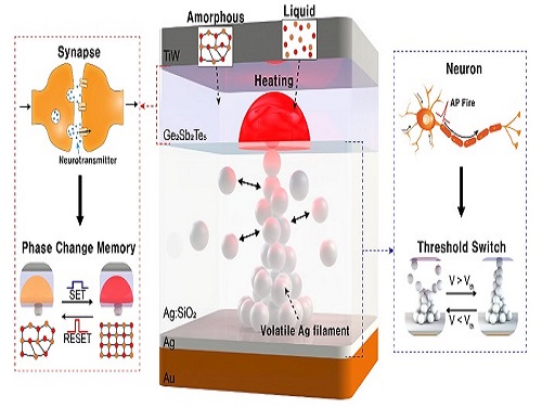
Researchers have reported a nano-sized neuromorphic memory device that emulates neurons and synapses simultaneously in a unit cell, another step toward completing the goal of neuromorphic computing designed to rigorously mimic the human brain with semiconductor devices.
Neuromorphic computing aims to realize artificial intelligence (AI) by mimicking the mechanisms of neurons and synapses that make up the human brain. Inspired by the cognitive functions of the human brain that current computers cannot provide, neuromorphic devices have been widely investigated. However, current Complementary Metal-Oxide Semiconductor (CMOS)-based neuromorphic circuits simply connect artificial neurons and synapses without synergistic interactions, and the concomitant implementation of neurons and synapses still remains a challenge. To address these issues, a research team led by Professor Keon Jae Lee from the Department of Materials Science and Engineering implemented the biological working mechanisms of humans by introducing the neuron-synapse interactions in a single memory cell, rather than the conventional approach of electrically connecting artificial neuronal and synaptic devices.
Similar to commercial graphics cards, the artificial synaptic devices previously studied often used to accelerate parallel computations, which shows clear differences from the operational mechanisms of the human brain. The research team implemented the synergistic interactions between neurons and synapses in the neuromorphic memory device, emulating the mechanisms of the biological neural network. In addition, the developed neuromorphic device can replace complex CMOS neuron circuits with a single device, providing high scalability and cost efficiency.
The human brain consists of a complex network of 100 billion neurons and 100 trillion synapses. The functions and structures of neurons and synapses can flexibly change according to the external stimuli, adapting to the surrounding environment. The research team developed a neuromorphic device in which short-term and long-term memories coexist using volatile and non-volatile memory devices that mimic the characteristics of neurons and synapses, respectively. A threshold switch device is used as volatile memory and phase-change memory is used as a non-volatile device. Two thin-film devices are integrated without intermediate electrodes, implementing the functional adaptability of neurons and synapses in the neuromorphic memory.
Professor Keon Jae Lee explained, "Neurons and synapses interact with each other to establish cognitive functions such as memory and learning, so simulating both is an essential element for brain-inspired artificial intelligence. The developed neuromorphic memory device also mimics the retraining effect that allows quick learning of the forgotten information by implementing a positive feedback effect between neurons and synapses.”
This result entitled “Simultaneous emulation of synaptic and intrinsic plasticity using a memristive synapse” was published in the May 19, 2022 issue of Nature Communications.
-Publication:Sang Hyun Sung, Tae Jin Kim, Hyera Shin, Tae Hong Im, and Keon Jae Lee (2022) “Simultaneous emulation of synaptic and intrinsic plasticity using a memristive synapse,” Nature Communications May 19, 2022 (DOI: 10.1038/s41467-022-30432-2)
-Profile:Professor Keon Jae Leehttp://fand.kaist.ac.kr
Department of Materials Science and EngineeringKAIST
2022.05.20 View 6536
Neuromorphic Memory Device Simulates Neurons and Synapses
Simultaneous emulation of neuronal and synaptic properties promotes the development of brain-like artificial intelligence
Researchers have reported a nano-sized neuromorphic memory device that emulates neurons and synapses simultaneously in a unit cell, another step toward completing the goal of neuromorphic computing designed to rigorously mimic the human brain with semiconductor devices.
Neuromorphic computing aims to realize artificial intelligence (AI) by mimicking the mechanisms of neurons and synapses that make up the human brain. Inspired by the cognitive functions of the human brain that current computers cannot provide, neuromorphic devices have been widely investigated. However, current Complementary Metal-Oxide Semiconductor (CMOS)-based neuromorphic circuits simply connect artificial neurons and synapses without synergistic interactions, and the concomitant implementation of neurons and synapses still remains a challenge. To address these issues, a research team led by Professor Keon Jae Lee from the Department of Materials Science and Engineering implemented the biological working mechanisms of humans by introducing the neuron-synapse interactions in a single memory cell, rather than the conventional approach of electrically connecting artificial neuronal and synaptic devices.
Similar to commercial graphics cards, the artificial synaptic devices previously studied often used to accelerate parallel computations, which shows clear differences from the operational mechanisms of the human brain. The research team implemented the synergistic interactions between neurons and synapses in the neuromorphic memory device, emulating the mechanisms of the biological neural network. In addition, the developed neuromorphic device can replace complex CMOS neuron circuits with a single device, providing high scalability and cost efficiency.
The human brain consists of a complex network of 100 billion neurons and 100 trillion synapses. The functions and structures of neurons and synapses can flexibly change according to the external stimuli, adapting to the surrounding environment. The research team developed a neuromorphic device in which short-term and long-term memories coexist using volatile and non-volatile memory devices that mimic the characteristics of neurons and synapses, respectively. A threshold switch device is used as volatile memory and phase-change memory is used as a non-volatile device. Two thin-film devices are integrated without intermediate electrodes, implementing the functional adaptability of neurons and synapses in the neuromorphic memory.
Professor Keon Jae Lee explained, "Neurons and synapses interact with each other to establish cognitive functions such as memory and learning, so simulating both is an essential element for brain-inspired artificial intelligence. The developed neuromorphic memory device also mimics the retraining effect that allows quick learning of the forgotten information by implementing a positive feedback effect between neurons and synapses.”
This result entitled “Simultaneous emulation of synaptic and intrinsic plasticity using a memristive synapse” was published in the May 19, 2022 issue of Nature Communications.
-Publication:Sang Hyun Sung, Tae Jin Kim, Hyera Shin, Tae Hong Im, and Keon Jae Lee (2022) “Simultaneous emulation of synaptic and intrinsic plasticity using a memristive synapse,” Nature Communications May 19, 2022 (DOI: 10.1038/s41467-022-30432-2)
-Profile:Professor Keon Jae Leehttp://fand.kaist.ac.kr
Department of Materials Science and EngineeringKAIST
2022.05.20 View 6536 -
 Industrial Liaison Program to Provide Comprehensive Consultation Services
The ILP’s one-stop solutions target all industrial sectors including conglomerates, small and medium-sized enterprises, venture companies, venture capital (VC) firms, and government-affiliated organizations.
The Industrial Liaison Center at KAIST launched the Industrial Liaison Program (ILP) on September 28, an industry-academic cooperation project to provide comprehensive solutions to industry partners. The Industrial Liaison Center will recruit member companies for this service every year, targeting all industrial sectors including conglomerates, small and medium-sized enterprises, venture companies, venture capital (VC) firms, and government-affiliated organizations.
The program plans to build a one-stop support system that can systematically share and use excellent resource information from KAIST’s research teams, R&D achievements, and infrastructure to provide member companies with much-needed services.
More than 40 KAIST professors with abundant academic-industrial collaboration experience will participate in the program. Experts from various fields with different points of view and experiences will jointly provide solutions to ILP member companies. To actively participate in academic-industrial liaisons and joint consultations, KAIST assigned 10 professors from related fields as program directors.
The program directors will come from four different fields including AI/robots (Professor Alice Oh, School from the School of Computing, Professor Young Jae Jang from the Department of Industrial & Systems Engineering, and Professor Yong-Hwa Park from Department of Mechanical Engineering), bio/medicine (Professor Daesoo Kim from Department of Biological Sciences and Professor YongKeun Park from Department of Physics), materials/electronics (Professor Sang Ouk Kim from the Department of Materials Science and Engineering and Professors Jun-Bo Yoon and Seonghwan Cho from the School of Electrical Engineering), and environment/energy (Professor Hee-Tak Kim from the Department of Biological Sciences and Professor Hoon Sohn from the Department of Civil and Environmental Engineering).
The transdisciplinary board of consulting professors that will lead technology innovation is composed of 30 professors including Professor Min-Soo Kim (School of Computing, AI), Professor Chan Hyuk Kim (Department of Biological Sciences, medicine), Professor Hae-Won Park (Department of Mechanical Engineering, robots), Professor Changho Suh (School of Electrical Engineering, electronics), Professor Haeshin Lee (Department of Chemistry, bio), Professor Il-Doo Kim (Department of Materials Science and Engineering, materials), Professor HyeJin Kim (School of Business Technology and Management), and Professor Byoung Pil Kim (School of Business Technology and Management, technology law)
The Head of the Industrial Liaison Center who is also in charge of the program, Professor Keon Jae Lee, said, “In a science and technology-oriented generation where technological supremacy determines national power, it is indispensable to build a new platform upon which innovative academic-industrial cooperation can be pushed forward in the fields of joint consultation, the development of academic-industrial projects, and the foundation of new industries.
He added, “KAIST professors carry out world-class research in many different fields and faculty members can come together through the ILP to communicate with representatives from industry to improve their corporations’ global competitiveness and further contribute to our nation’s interests by cultivating strong small enterprises
2021.09.30 View 3847
Industrial Liaison Program to Provide Comprehensive Consultation Services
The ILP’s one-stop solutions target all industrial sectors including conglomerates, small and medium-sized enterprises, venture companies, venture capital (VC) firms, and government-affiliated organizations.
The Industrial Liaison Center at KAIST launched the Industrial Liaison Program (ILP) on September 28, an industry-academic cooperation project to provide comprehensive solutions to industry partners. The Industrial Liaison Center will recruit member companies for this service every year, targeting all industrial sectors including conglomerates, small and medium-sized enterprises, venture companies, venture capital (VC) firms, and government-affiliated organizations.
The program plans to build a one-stop support system that can systematically share and use excellent resource information from KAIST’s research teams, R&D achievements, and infrastructure to provide member companies with much-needed services.
More than 40 KAIST professors with abundant academic-industrial collaboration experience will participate in the program. Experts from various fields with different points of view and experiences will jointly provide solutions to ILP member companies. To actively participate in academic-industrial liaisons and joint consultations, KAIST assigned 10 professors from related fields as program directors.
The program directors will come from four different fields including AI/robots (Professor Alice Oh, School from the School of Computing, Professor Young Jae Jang from the Department of Industrial & Systems Engineering, and Professor Yong-Hwa Park from Department of Mechanical Engineering), bio/medicine (Professor Daesoo Kim from Department of Biological Sciences and Professor YongKeun Park from Department of Physics), materials/electronics (Professor Sang Ouk Kim from the Department of Materials Science and Engineering and Professors Jun-Bo Yoon and Seonghwan Cho from the School of Electrical Engineering), and environment/energy (Professor Hee-Tak Kim from the Department of Biological Sciences and Professor Hoon Sohn from the Department of Civil and Environmental Engineering).
The transdisciplinary board of consulting professors that will lead technology innovation is composed of 30 professors including Professor Min-Soo Kim (School of Computing, AI), Professor Chan Hyuk Kim (Department of Biological Sciences, medicine), Professor Hae-Won Park (Department of Mechanical Engineering, robots), Professor Changho Suh (School of Electrical Engineering, electronics), Professor Haeshin Lee (Department of Chemistry, bio), Professor Il-Doo Kim (Department of Materials Science and Engineering, materials), Professor HyeJin Kim (School of Business Technology and Management), and Professor Byoung Pil Kim (School of Business Technology and Management, technology law)
The Head of the Industrial Liaison Center who is also in charge of the program, Professor Keon Jae Lee, said, “In a science and technology-oriented generation where technological supremacy determines national power, it is indispensable to build a new platform upon which innovative academic-industrial cooperation can be pushed forward in the fields of joint consultation, the development of academic-industrial projects, and the foundation of new industries.
He added, “KAIST professors carry out world-class research in many different fields and faculty members can come together through the ILP to communicate with representatives from industry to improve their corporations’ global competitiveness and further contribute to our nation’s interests by cultivating strong small enterprises
2021.09.30 View 3847 -
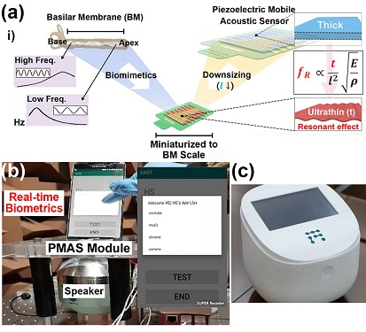 Biomimetic Resonant Acoustic Sensor Detecting Far-Distant Voices Accurately to Hit the Market
A KAIST research team led by Professor Keon Jae Lee from the Department of Materials Science and Engineering has developed a bioinspired flexible piezoelectric acoustic sensor with multi-resonant ultrathin piezoelectric membrane mimicking the basilar membrane of the human cochlea. The flexible acoustic sensor has been miniaturized for embedding into smartphones and the first commercial prototype is ready for accurate and far-distant voice detection.
In 2018, Professor Lee presented the first concept of a flexible piezoelectric acoustic sensor, inspired by the fact that humans can accurately detect far-distant voices using a multi-resonant trapezoidal membrane with 20,000 hair cells. However, previous acoustic sensors could not be integrated into commercial products like smartphones and AI speakers due to their large device size.
In this work, the research team fabricated a mobile-sized acoustic sensor by adopting ultrathin piezoelectric membranes with high sensitivity. Simulation studies proved that the ultrathin polymer underneath inorganic piezoelectric thin film can broaden the resonant bandwidth to cover the entire voice frequency range using seven channels. Based on this theory, the research team successfully demonstrated the miniaturized acoustic sensor mounted in commercial smartphones and AI speakers for machine learning-based biometric authentication and voice processing. (Please refer to the explanatory movie KAIST Flexible Piezoelectric Mobile Acoustic Sensor).
The resonant mobile acoustic sensor has superior sensitivity and multi-channel signals compared to conventional condenser microphones with a single channel, and it has shown highly accurate and far-distant speaker identification with a small amount of voice training data. The error rate of speaker identification was significantly reduced by 56% (with 150 training datasets) and 75% (with 2,800 training datasets) compared to that of a MEMS condenser device.
Professor Lee said, “Recently, Google has been targeting the ‘Wolverine Project’ on far-distant voice separation from multi-users for next-generation AI user interfaces. I expect that our multi-channel resonant acoustic sensor with abundant voice information is the best fit for this application. Currently, the mass production process is on the verge of completion, so we hope that this will be used in our daily lives very soon.”
Professor Lee also established a startup company called Fronics Inc., located both in Korea and U.S. (branch office) to commercialize this flexible acoustic sensor and is seeking collaborations with global AI companies.
These research results entitled “Biomimetic and Flexible Piezoelectric Mobile Acoustic Sensors with Multi-Resonant Ultrathin Structures for Machine Learning Biometrics” were published in Science Advances in 2021 (7, eabe5683).
-Publication
“Biomimetic and flexible piezoelectric mobile acoustic sensors with multiresonant ultrathin structures for machine learning biometrics,” Science Advances (DOI: 10.1126/sciadv.abe5683)
-Profile
Professor Keon Jae Lee
Department of Materials Science and Engineering
Flexible and Nanobio Device Lab
http://fand.kaist.ac.kr/
KAIST
2021.06.14 View 6350
Biomimetic Resonant Acoustic Sensor Detecting Far-Distant Voices Accurately to Hit the Market
A KAIST research team led by Professor Keon Jae Lee from the Department of Materials Science and Engineering has developed a bioinspired flexible piezoelectric acoustic sensor with multi-resonant ultrathin piezoelectric membrane mimicking the basilar membrane of the human cochlea. The flexible acoustic sensor has been miniaturized for embedding into smartphones and the first commercial prototype is ready for accurate and far-distant voice detection.
In 2018, Professor Lee presented the first concept of a flexible piezoelectric acoustic sensor, inspired by the fact that humans can accurately detect far-distant voices using a multi-resonant trapezoidal membrane with 20,000 hair cells. However, previous acoustic sensors could not be integrated into commercial products like smartphones and AI speakers due to their large device size.
In this work, the research team fabricated a mobile-sized acoustic sensor by adopting ultrathin piezoelectric membranes with high sensitivity. Simulation studies proved that the ultrathin polymer underneath inorganic piezoelectric thin film can broaden the resonant bandwidth to cover the entire voice frequency range using seven channels. Based on this theory, the research team successfully demonstrated the miniaturized acoustic sensor mounted in commercial smartphones and AI speakers for machine learning-based biometric authentication and voice processing. (Please refer to the explanatory movie KAIST Flexible Piezoelectric Mobile Acoustic Sensor).
The resonant mobile acoustic sensor has superior sensitivity and multi-channel signals compared to conventional condenser microphones with a single channel, and it has shown highly accurate and far-distant speaker identification with a small amount of voice training data. The error rate of speaker identification was significantly reduced by 56% (with 150 training datasets) and 75% (with 2,800 training datasets) compared to that of a MEMS condenser device.
Professor Lee said, “Recently, Google has been targeting the ‘Wolverine Project’ on far-distant voice separation from multi-users for next-generation AI user interfaces. I expect that our multi-channel resonant acoustic sensor with abundant voice information is the best fit for this application. Currently, the mass production process is on the verge of completion, so we hope that this will be used in our daily lives very soon.”
Professor Lee also established a startup company called Fronics Inc., located both in Korea and U.S. (branch office) to commercialize this flexible acoustic sensor and is seeking collaborations with global AI companies.
These research results entitled “Biomimetic and Flexible Piezoelectric Mobile Acoustic Sensors with Multi-Resonant Ultrathin Structures for Machine Learning Biometrics” were published in Science Advances in 2021 (7, eabe5683).
-Publication
“Biomimetic and flexible piezoelectric mobile acoustic sensors with multiresonant ultrathin structures for machine learning biometrics,” Science Advances (DOI: 10.1126/sciadv.abe5683)
-Profile
Professor Keon Jae Lee
Department of Materials Science and Engineering
Flexible and Nanobio Device Lab
http://fand.kaist.ac.kr/
KAIST
2021.06.14 View 6350 -
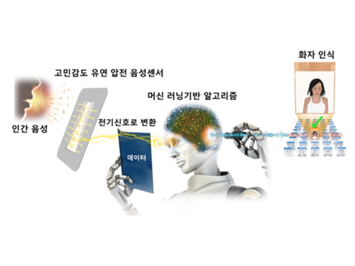 Flexible Piezoelectric Acoustic Sensors for Speaker Recognition
A KAIST research team led by Professor Keon Jae Lee from the Department of Material Science and Engineering has developed a machine learning-based acoustic sensor for speaker recognition.
Acoustic sensors were spotlighted as one of the most intuitive bilateral communication devices between humans and machines. However, conventional acoustic sensors use a condenser-type device for measuring capacitance between two conducting layers, resulting in low sensitivity, short recognition distance, and low speaker recognition rates.
The team fabricated a flexible piezoelectric membrane by mimicking the basilar membrane in the human cochlear. Resonant frequencies vibrate corresponding regions of the trapezoidal piezoelectric membrane, which converts voice to electrical signal with a highly sensitive self-powered acoustic sensor.
This multi-channel piezoelectric acoustic sensor exhibits sensitivity more than two times higher and allows for more abundant voice information compared to conventional acoustic sensors, which can detect minute sounds from farther distances. In addition, the acoustic sensor can achieve a 97.5% speaker recognition rate using a machine learning algorithm, reducing by 75% error rate than the reference microphone.
AI speaker recognition is the next big thing for future individual customized services. However, conventional technology attempts to improve recognition rates by using software upgrades, resulting in limited speaker recognition rates. The team enhanced the speaker recognition system by replacing the existing hardware with an innovative flexible piezoelectric acoustic sensor. Further software improvement of the piezoelectric acoustic sensor will significantly increase the speaker and voice recognition rate in diverse environments.
Professor Lee said, “Highly sensitive self-powered acoustic sensors for speaker recognition can be used for personalized voice services such as smart home appliances, AI secretaries, always-on IoT, biometric authentication, and FinTech.”
These research “Basilar Membrane-Inspired Self-Powered Acoustic Sensor” and “Machine Learning-based Acoustic Sensor for Speaker Recognition” were published in the September 2018 issue of Nano Energy.
Firgure 1: A flexible piezoelectric acoustic sensor mimicking the human cochlear.
Figure 2: Speaker recognition with a machine learning algorithm.
2018.10.04 View 5828
Flexible Piezoelectric Acoustic Sensors for Speaker Recognition
A KAIST research team led by Professor Keon Jae Lee from the Department of Material Science and Engineering has developed a machine learning-based acoustic sensor for speaker recognition.
Acoustic sensors were spotlighted as one of the most intuitive bilateral communication devices between humans and machines. However, conventional acoustic sensors use a condenser-type device for measuring capacitance between two conducting layers, resulting in low sensitivity, short recognition distance, and low speaker recognition rates.
The team fabricated a flexible piezoelectric membrane by mimicking the basilar membrane in the human cochlear. Resonant frequencies vibrate corresponding regions of the trapezoidal piezoelectric membrane, which converts voice to electrical signal with a highly sensitive self-powered acoustic sensor.
This multi-channel piezoelectric acoustic sensor exhibits sensitivity more than two times higher and allows for more abundant voice information compared to conventional acoustic sensors, which can detect minute sounds from farther distances. In addition, the acoustic sensor can achieve a 97.5% speaker recognition rate using a machine learning algorithm, reducing by 75% error rate than the reference microphone.
AI speaker recognition is the next big thing for future individual customized services. However, conventional technology attempts to improve recognition rates by using software upgrades, resulting in limited speaker recognition rates. The team enhanced the speaker recognition system by replacing the existing hardware with an innovative flexible piezoelectric acoustic sensor. Further software improvement of the piezoelectric acoustic sensor will significantly increase the speaker and voice recognition rate in diverse environments.
Professor Lee said, “Highly sensitive self-powered acoustic sensors for speaker recognition can be used for personalized voice services such as smart home appliances, AI secretaries, always-on IoT, biometric authentication, and FinTech.”
These research “Basilar Membrane-Inspired Self-Powered Acoustic Sensor” and “Machine Learning-based Acoustic Sensor for Speaker Recognition” were published in the September 2018 issue of Nano Energy.
Firgure 1: A flexible piezoelectric acoustic sensor mimicking the human cochlear.
Figure 2: Speaker recognition with a machine learning algorithm.
2018.10.04 View 5828 -
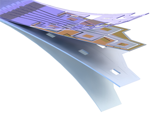 Flexible Drug Delivery Microdevice to Advance Precision Medicine
(Schematic view of flexible microdevice: The flexible drug delivery device for controlled release fabricated via inorganic laser lift off.)
A KAIST research team has developed a flexible drug delivery device with controlled release for personalized medicine, blazing the path toward theragnosis.
Theragnosis, an emerging medical technology, is gaining attention as key factor to advance precision medicine for its featuring simultaneous diagnosis and therapeutics. Theragnosis devices including smart contact lenses and microneedle patches integrate physiological data sensors and drug delivery devices. The controlled drug delivery boasts fewer side-effects, uniform therapeutic results, and minimal dosages compared to oral ingestion. Recently, some research groups conducted in-human applications of controlled-release bulky microchips for osteoporosis treatment. However they failed to demonstrate successful human-friendly flexible drug delivery systems for controlled release.
For this microdevice, the team under Professor Daesoo Kim from the Department of Biological Science and Professor Keon Jae Lee from the Department of Materials Science and Engineering, fabricated a device on a rigid substrate and transferred a 50 µm-thick active drug delivery layer to the flexible substrate via inorganic laser lift off. The fabricated device shows mechanical flexibility while maintaining the capability of precise administration of exact dosages at desired times. The core technology is to produce a freestanding gold capping layer directly on top of the microreservoir with the drugs inside, which had been regarded as impossible in conventional microfabrication.
The developed flexible drug delivery system can be applied to smart contact lenses or the brain disease treatments by implanting them into cramped and corrugated organs. In addition, when powered wirelessly, it will represent a novel platform for personalized medicine. The team already proved through animal experimentation that treatment for brain epilepsy made progress by releasing anti-epileptic medication through the device.
Professor Lee believes the flexible microdevice will further expand the applications of smart contact lenses, therapeutic treatments for brain disease, and subcutaneous implantations for daily healthcare system. This study “Flexible Wireless Powered Drug Delivery System for Targeted Administration on Cerebral Cortex” was described in the June online issue of Nano Energy.
(Photo: The flexible drug delivery device for contolled relase attached on a glass rod.)
2018.08.13 View 7072
Flexible Drug Delivery Microdevice to Advance Precision Medicine
(Schematic view of flexible microdevice: The flexible drug delivery device for controlled release fabricated via inorganic laser lift off.)
A KAIST research team has developed a flexible drug delivery device with controlled release for personalized medicine, blazing the path toward theragnosis.
Theragnosis, an emerging medical technology, is gaining attention as key factor to advance precision medicine for its featuring simultaneous diagnosis and therapeutics. Theragnosis devices including smart contact lenses and microneedle patches integrate physiological data sensors and drug delivery devices. The controlled drug delivery boasts fewer side-effects, uniform therapeutic results, and minimal dosages compared to oral ingestion. Recently, some research groups conducted in-human applications of controlled-release bulky microchips for osteoporosis treatment. However they failed to demonstrate successful human-friendly flexible drug delivery systems for controlled release.
For this microdevice, the team under Professor Daesoo Kim from the Department of Biological Science and Professor Keon Jae Lee from the Department of Materials Science and Engineering, fabricated a device on a rigid substrate and transferred a 50 µm-thick active drug delivery layer to the flexible substrate via inorganic laser lift off. The fabricated device shows mechanical flexibility while maintaining the capability of precise administration of exact dosages at desired times. The core technology is to produce a freestanding gold capping layer directly on top of the microreservoir with the drugs inside, which had been regarded as impossible in conventional microfabrication.
The developed flexible drug delivery system can be applied to smart contact lenses or the brain disease treatments by implanting them into cramped and corrugated organs. In addition, when powered wirelessly, it will represent a novel platform for personalized medicine. The team already proved through animal experimentation that treatment for brain epilepsy made progress by releasing anti-epileptic medication through the device.
Professor Lee believes the flexible microdevice will further expand the applications of smart contact lenses, therapeutic treatments for brain disease, and subcutaneous implantations for daily healthcare system. This study “Flexible Wireless Powered Drug Delivery System for Targeted Administration on Cerebral Cortex” was described in the June online issue of Nano Energy.
(Photo: The flexible drug delivery device for contolled relase attached on a glass rod.)
2018.08.13 View 7072 -
 KAIST Team Develops Flexible Blue Vertical Micro LEDs
A KAIST research team developed a crucial source technology that will advance the commercialization of micro LEDs.
Professor Keon Jae Lee from the Department of Materials Science and Engineering and his team have developed a low cost production technology for thin-film blue flexible vertical micro LEDs (f-VLEDs).
In CES 2018, micro LED TV was spotlighted as a strong candidate for replacing the active-matrix organic light-emitting diode (AMOLED) display. Micro LED is a sub-100 um light source for red, green and blue light, which has advantages of outstanding optical output, ultra-low power consumption, fast response speed, and excellent flexibility.
However, the current display industry has utilized the individual chip transfer of millions of LED pixels, causing high production cost. Therefore, the initial market of micro LED TV will be estimated to ~ a hundred thousand dollars for global premium market.
To widely commercialize micro LEDs for mobile and TV displays, the transfer method of thin film micro LEDs requires a one-time transfer of one million LEDs. In addition, highly efficient thin-film blue micro LED is crucial for a full-color display.
The team developed thin-film red f-VLED in previous projects, and now has realized thousands of thin-film blue vertical micro LEDs (thickness < 2 μm) on plastics using a one-time transfer.
The blue GaN f-VLEDs achieved optical power density (~30 mW/mm2) three times higher than that of lateral micro LEDs, and a device lifetime of 100,000 hours by reducing heat generation. These blue f-VLEDs could be conformally attached to the curved skin and brains for wearable devices, and stably operated by wirelessly transferred electrical energy.
Professor Lee said, “For future micro LEDs, the innovative technology of thin-film transfer, efficient devices, and interconnection is necessary. We plan to demonstrate a full-color micro LED display in smart watch sizes by the end of this year. ”
This research “ Monolithic Flexible Vertical GaN Light‐Emitting Diodes for a Transparent Wireless Brain Optical Stimulator ” led by a PhD candidate Han Eol Lee was published in the June 2018 issue of Advanced Materials.
Figure 1. Schematic image of wireless thin-film blue f-VLED arrays on the brain surface
Figure 2. Photo of high-performance and high-density blue f-VLED arrays
2018.06.18 View 7464
KAIST Team Develops Flexible Blue Vertical Micro LEDs
A KAIST research team developed a crucial source technology that will advance the commercialization of micro LEDs.
Professor Keon Jae Lee from the Department of Materials Science and Engineering and his team have developed a low cost production technology for thin-film blue flexible vertical micro LEDs (f-VLEDs).
In CES 2018, micro LED TV was spotlighted as a strong candidate for replacing the active-matrix organic light-emitting diode (AMOLED) display. Micro LED is a sub-100 um light source for red, green and blue light, which has advantages of outstanding optical output, ultra-low power consumption, fast response speed, and excellent flexibility.
However, the current display industry has utilized the individual chip transfer of millions of LED pixels, causing high production cost. Therefore, the initial market of micro LED TV will be estimated to ~ a hundred thousand dollars for global premium market.
To widely commercialize micro LEDs for mobile and TV displays, the transfer method of thin film micro LEDs requires a one-time transfer of one million LEDs. In addition, highly efficient thin-film blue micro LED is crucial for a full-color display.
The team developed thin-film red f-VLED in previous projects, and now has realized thousands of thin-film blue vertical micro LEDs (thickness < 2 μm) on plastics using a one-time transfer.
The blue GaN f-VLEDs achieved optical power density (~30 mW/mm2) three times higher than that of lateral micro LEDs, and a device lifetime of 100,000 hours by reducing heat generation. These blue f-VLEDs could be conformally attached to the curved skin and brains for wearable devices, and stably operated by wirelessly transferred electrical energy.
Professor Lee said, “For future micro LEDs, the innovative technology of thin-film transfer, efficient devices, and interconnection is necessary. We plan to demonstrate a full-color micro LED display in smart watch sizes by the end of this year. ”
This research “ Monolithic Flexible Vertical GaN Light‐Emitting Diodes for a Transparent Wireless Brain Optical Stimulator ” led by a PhD candidate Han Eol Lee was published in the June 2018 issue of Advanced Materials.
Figure 1. Schematic image of wireless thin-film blue f-VLED arrays on the brain surface
Figure 2. Photo of high-performance and high-density blue f-VLED arrays
2018.06.18 View 7464 -
 KAIST Professors Selected as Y-KAST Members
Professor YongKeun Park, Professor Bumjoon Kim, Professor Keon Jae Lee, and Professor Young Seok Ju were selected as the newest members of the Young Korean Academy of Science and Technology (Y-KAST).
The Korean Academy of Science and Technology, an academic institution of professional experts, selected 26 promising scientists under the age of 43 to join Y-KAST. and four KAIST professors were included in the list.
The newest members were conferred on February 26.
Research Field
Name
Natural Sciences
YongKeun Park (Dept. of Physics)
Engineering
Bumjoon Kim (Dept. of Chemical and Biomolecular Engineering)
Agricultural & Fishery Sciences
Keon Jae Lee (Dept. of Materials Science and Engineering)
Medical Sciences
Young Seok Ju (Graduate School of Medical Science and Engineering)
2018.03.05 View 6434
KAIST Professors Selected as Y-KAST Members
Professor YongKeun Park, Professor Bumjoon Kim, Professor Keon Jae Lee, and Professor Young Seok Ju were selected as the newest members of the Young Korean Academy of Science and Technology (Y-KAST).
The Korean Academy of Science and Technology, an academic institution of professional experts, selected 26 promising scientists under the age of 43 to join Y-KAST. and four KAIST professors were included in the list.
The newest members were conferred on February 26.
Research Field
Name
Natural Sciences
YongKeun Park (Dept. of Physics)
Engineering
Bumjoon Kim (Dept. of Chemical and Biomolecular Engineering)
Agricultural & Fishery Sciences
Keon Jae Lee (Dept. of Materials Science and Engineering)
Medical Sciences
Young Seok Ju (Graduate School of Medical Science and Engineering)
2018.03.05 View 6434 -
 Developing Flexible Vertical Micro LED
A KAIST research team led by Professor Keon Jae Lee from the Department of Materials Science and Engineering and Professor Daesoo Kim from the Department of Biological Sciences has developed flexible vertical micro LEDs (f-VLEDs) using anisotropic conductive film (ACF)-based transfer and interconnection technology. The team also succeeded in controlling animal behavior via optogenetic stimulation of the f-VLEDs.
Flexible micro LEDs have become a strong candidate for the next-generation display due to their ultra-low power consumption, fast response speed, and excellent flexibility. However, the previous micro LED technology had critical issues such as poor device efficiency, low thermal reliability, and the lack of interconnection technology for high-resolution micro LED displays.
The research team has designed new transfer equipment and fabricated a f-VLED array (50ⅹ50) using simultaneous transfer and interconnection through the precise alignment of ACF bonding process. These f-VLEDs (thickness: 5 ㎛, size: below 80 ㎛) achieved optical power density (30 mW/mm2) three times higher than that of lateral micro LEDs, improving thermal reliability and lifetime by reducing heat generation within the thin film LEDs.
These f-VLEDs can be applied to optogenetics for controlling the behavior of neuron cells and brains. In contrast to the electrical stimulation that activates all of the neurons in brain, optogenetics can stimulate specific excitatory or inhibitory neurons within the localized cortical areas of the brain, which facilitates precise analysis, high-resolution mapping, and neuron modulation of animal brains. (Refer to the author’s previous ACS Nano paper of “Optogenetic Mapping of Functional Connectivity in Freely Moving Mice via Insertable Wrapping Electrode Array Beneath the Skull.” )
In this work, they inserted the innovative f-VLEDs into the narrow space between the skull and the brain surface and succeeded in controlling mouse behavior by illuminating motor neurons on two-dimensional cortical areas located deep below the brain surface.
Professor Lee said, “The flexible vertical micro LED can be used in low-power smart watches, mobile displays, and wearable lighting. In addition, these flexible optoelectronic devices are suitable for biomedical applications such as brain science, phototherapeutic treatment, and contact lens biosensors.”
He recently established a startup company ( FRONICS Inc. ) based on micro LED technology and is looking for global partnerships for commercialization. This result entitled “ Optogenetic Control of Body Movements via Flexible Vertical Light-Emitting Diodes on Brain Surface ” was published in the February 2018 issue of Nano Energy.
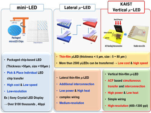
Figure 1. Comparison of μ-LEDs Technology
2018.01.29 View 10480
Developing Flexible Vertical Micro LED
A KAIST research team led by Professor Keon Jae Lee from the Department of Materials Science and Engineering and Professor Daesoo Kim from the Department of Biological Sciences has developed flexible vertical micro LEDs (f-VLEDs) using anisotropic conductive film (ACF)-based transfer and interconnection technology. The team also succeeded in controlling animal behavior via optogenetic stimulation of the f-VLEDs.
Flexible micro LEDs have become a strong candidate for the next-generation display due to their ultra-low power consumption, fast response speed, and excellent flexibility. However, the previous micro LED technology had critical issues such as poor device efficiency, low thermal reliability, and the lack of interconnection technology for high-resolution micro LED displays.
The research team has designed new transfer equipment and fabricated a f-VLED array (50ⅹ50) using simultaneous transfer and interconnection through the precise alignment of ACF bonding process. These f-VLEDs (thickness: 5 ㎛, size: below 80 ㎛) achieved optical power density (30 mW/mm2) three times higher than that of lateral micro LEDs, improving thermal reliability and lifetime by reducing heat generation within the thin film LEDs.
These f-VLEDs can be applied to optogenetics for controlling the behavior of neuron cells and brains. In contrast to the electrical stimulation that activates all of the neurons in brain, optogenetics can stimulate specific excitatory or inhibitory neurons within the localized cortical areas of the brain, which facilitates precise analysis, high-resolution mapping, and neuron modulation of animal brains. (Refer to the author’s previous ACS Nano paper of “Optogenetic Mapping of Functional Connectivity in Freely Moving Mice via Insertable Wrapping Electrode Array Beneath the Skull.” )
In this work, they inserted the innovative f-VLEDs into the narrow space between the skull and the brain surface and succeeded in controlling mouse behavior by illuminating motor neurons on two-dimensional cortical areas located deep below the brain surface.
Professor Lee said, “The flexible vertical micro LED can be used in low-power smart watches, mobile displays, and wearable lighting. In addition, these flexible optoelectronic devices are suitable for biomedical applications such as brain science, phototherapeutic treatment, and contact lens biosensors.”
He recently established a startup company ( FRONICS Inc. ) based on micro LED technology and is looking for global partnerships for commercialization. This result entitled “ Optogenetic Control of Body Movements via Flexible Vertical Light-Emitting Diodes on Brain Surface ” was published in the February 2018 issue of Nano Energy.
Figure 1. Comparison of μ-LEDs Technology
2018.01.29 View 10480 -
 Semiconductor Patterning of Seven Nanometers Technology Using a Camera Flash
A research team led by Professor Sang Ouk Kim in the Department of Materials Science and Engineering at KAIST has developed semiconductor manufacturing technology using a camera flash.
This technology can manufacture ultra-fine patterns over a large area by irradiating a single flash with a seven-nanometer patterning technique for semiconductors. It can facilitate the manufacturing of highly efficient, integrated semiconductor devices in the future.
Technology for the Artificial Intelligence (AI), the Internet of Things (IoTs), and big data, which are the major keys for the fourth Industrial Revolution, require high-capacity, high-performance semiconductor devices. It is necessary to develop lithography technology to produce such next-generation, highly integrated semiconductor devices.
Although related industries have been using conventional photolithography for small patterns, this technique has limitations for forming a pattern of sub-10 nm patterns.
Molecular assembly patterning technology using polymers has been in the spotlight as the next generation technology to replace photolithography because it is inexpensive to produce and can easily form sub-10 nm patterns. However, since it generally takes a long time for heat treatment at high-temperature or toxic solvent vapor treatment, mass production is difficult and thus its commercialization has been limited.
The research team introduced a camera flash that instantly emits strong light to solve the issues of polymer molecular assembly patterning. Using a flash can possibly achieve a semiconductor patterning of seven nanometers within 15 milliseconds (1 millisecond = 1/1,000 second), which can generate a temperature of several hundred degrees Celsius in several tens of milliseconds.
The team has demonstrated that applying this technology to polymer molecular assembly allows a single flash of light to form molecular assembly patterns.
The team also identified its compatibility with polymer flexible substrates, which are impossible to process at high temperatures. Through these findings, the technology can be applied to the fabrication of next-generation, flexible semiconductors.
The researchers said the camera flash photo-thermal process will be introduced into molecular assembly technology and this highly-efficiency technology can accelerate the realization of molecular assembly semiconductor technology.
Professor Kim, who led the research, said, “Despite its potential, molecular assembly semiconductor technology has remained a big challenge in improving process efficiency.” “This technology will be a breakthrough for the practical use of molecular assembly-based semiconductors.”
The paper was published in the international journal, Advanced Materials on August 21 with first authors, researcher Hyeong Min Jin and PhD candidate Dae Yong Park.
The research, sponsored by the Ministry of Science and ICT, was co-led Professor by Keon Jae Lee in the Department of Materials Science and Engineering at KAIST, and Professor Kwang Ho Kim in the School of Materials Science and Engineering at Pusan National University.
(1. Formation of semiconductor patterns using a camera flash)
(Schematic diagram of molecular assembly pattern using a camera flash)
(Self-assembled patterns)
2017.09.18 View 8598
Semiconductor Patterning of Seven Nanometers Technology Using a Camera Flash
A research team led by Professor Sang Ouk Kim in the Department of Materials Science and Engineering at KAIST has developed semiconductor manufacturing technology using a camera flash.
This technology can manufacture ultra-fine patterns over a large area by irradiating a single flash with a seven-nanometer patterning technique for semiconductors. It can facilitate the manufacturing of highly efficient, integrated semiconductor devices in the future.
Technology for the Artificial Intelligence (AI), the Internet of Things (IoTs), and big data, which are the major keys for the fourth Industrial Revolution, require high-capacity, high-performance semiconductor devices. It is necessary to develop lithography technology to produce such next-generation, highly integrated semiconductor devices.
Although related industries have been using conventional photolithography for small patterns, this technique has limitations for forming a pattern of sub-10 nm patterns.
Molecular assembly patterning technology using polymers has been in the spotlight as the next generation technology to replace photolithography because it is inexpensive to produce and can easily form sub-10 nm patterns. However, since it generally takes a long time for heat treatment at high-temperature or toxic solvent vapor treatment, mass production is difficult and thus its commercialization has been limited.
The research team introduced a camera flash that instantly emits strong light to solve the issues of polymer molecular assembly patterning. Using a flash can possibly achieve a semiconductor patterning of seven nanometers within 15 milliseconds (1 millisecond = 1/1,000 second), which can generate a temperature of several hundred degrees Celsius in several tens of milliseconds.
The team has demonstrated that applying this technology to polymer molecular assembly allows a single flash of light to form molecular assembly patterns.
The team also identified its compatibility with polymer flexible substrates, which are impossible to process at high temperatures. Through these findings, the technology can be applied to the fabrication of next-generation, flexible semiconductors.
The researchers said the camera flash photo-thermal process will be introduced into molecular assembly technology and this highly-efficiency technology can accelerate the realization of molecular assembly semiconductor technology.
Professor Kim, who led the research, said, “Despite its potential, molecular assembly semiconductor technology has remained a big challenge in improving process efficiency.” “This technology will be a breakthrough for the practical use of molecular assembly-based semiconductors.”
The paper was published in the international journal, Advanced Materials on August 21 with first authors, researcher Hyeong Min Jin and PhD candidate Dae Yong Park.
The research, sponsored by the Ministry of Science and ICT, was co-led Professor by Keon Jae Lee in the Department of Materials Science and Engineering at KAIST, and Professor Kwang Ho Kim in the School of Materials Science and Engineering at Pusan National University.
(1. Formation of semiconductor patterns using a camera flash)
(Schematic diagram of molecular assembly pattern using a camera flash)
(Self-assembled patterns)
2017.09.18 View 8598